Hi all,
I am working on a very simple design (basically a CMOS inverter) using Virtuoso IC6.1.5 with AMS C35B4C3 PDK.
I included seven ground pins/pads (for GSG RF probes) that are wired together (labelled "MASSE" on the schematic) :

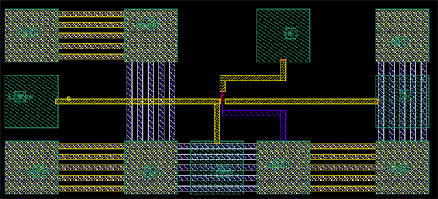
The corresponding layout of course includes these pads, tied together using metal strips (be forgiving, it's an experimental layout) :

In this configuration, DRC and LVS are passed with no errors, and I can make QRC parasitic extraction without problems
However, I'd like to be able to "separate" these ground pins both on the schematic and layout since, in layout, interconnects between these pins through the metal strips introduce parasitic resistances (at least) and inductances that physically make the different pads non equipotential, especially at RF frequencies.
And I need to be able to identify each of these pins with regards to its location on the layout : for instance, the upper left one is connected to the lower right one through a path that is not the same as the lower left-upper left connection. But the extracted layout does not allow me to tell which pin is what...
I've tried to make these pins distinct by assigning a different name to each of them on the schematic, and naming the electrical connections for correct tapping, but LVS fails since it sees shorts between the pins, and this does not allow me to run the QRC parasitic extraction.
So I do not know how to solve this. It's quite similar problem to the one described here :
but the DK I use does not have metal resistors too, and the post gives no solution.
Thanks in advance for any information or correction.
Best,
François