Thanks in advance for helping me with this issue:
I have a problem with the extracted view of a simple NAND circuit. I am using IC 6.1.8, running the LVS with PVS (19.10) and the extraction with Quantus (19.13). The PDK I am using is the GPDK045 provided by Cadence as a generic 45nm process design kit.
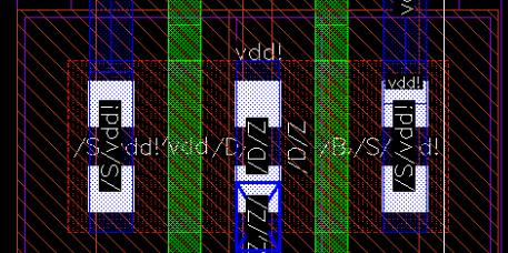
The layout of my NAND has 2 PMOS with a shared drain as shown in Figure (the central node):

The shared drain diffusion has an area of 38.4E-15m2 (240nm x 160nm). After running the extraction I checked the extracted netlist which looks like this:

Both the drain area of M3 and M4 (the 2 PMOS transistors) is calculated as being equal to the area of the shared drain diffusion. In this way, the corresponding parasitic capacitance is counted twice in simulation, as far as I understand.
Is there something I am missing or some checkbox I should tick setting up the extraction?
Thank you in advance and best regards